Engineer Interviews
Semiconductors that Solve Issues
Epson's semiconductor business has developed original device technology that drives primarily from the
efficient, compact, and precision technologies that Epson initially developed for wristwatch
semiconductors. The semiconductor business provides chips for use in Epson's finished products, thus
increasing their value. The company also applies this technology to support outside
customers.
Epson's semiconductor business has many different technologies and products, including
semiconductors for in-vehicle applications. We interviewed a senior engineer involved in the development
of ICs for these latter systems about product features, future prospects, and his thoughts on development.
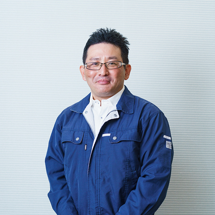
IC Product Development Department
Yamada
Developing semiconductors in close partnership with customers
Many people associate Epson with printers, so how did Epson get involved in semiconductor technology development and product development?
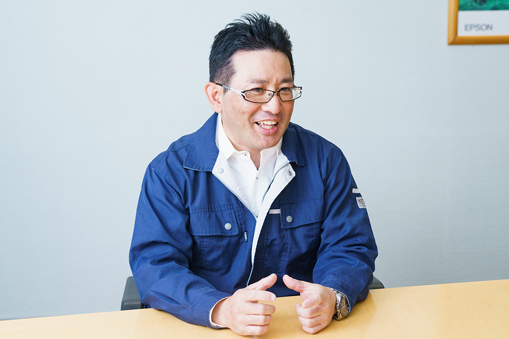
YamadaEpson's history in semiconductor development is closely tied to watch development. This is because it was essential to incorporate semiconductor technology into watches to reduce power consumption, make them smaller, and stabilize crystal oscillation to commercialize the world's first quartz watch. Since then, we have been developing semiconductors to support Epson's finished products, such as LCDs, printers, scanners, projectors, and robots. Epson's strengths as a manufacturer lie in what we call our efficient, compact and precision technologies, and we seek to make Epson semiconductors the foundation of this technology.
In addition to semiconductor circuits for internal customers, we also sell crystal oscillators, MCUs, LCD drivers, LCD controllers, USB communications ICs and other semiconductor products to external customers. An Epson semiconductor may even be inside a product you are using.
Tell us about the products you work on and their features.
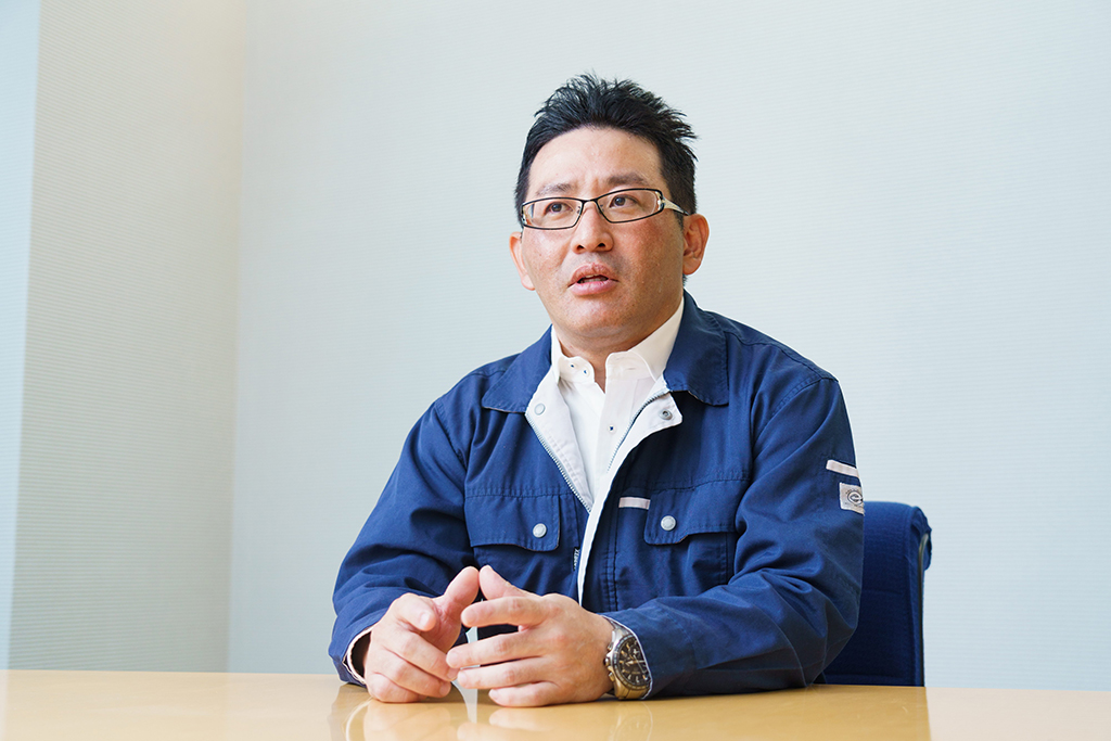
YamadaI develop semiconductor products for in-vehicle applications. Recently, we are working on the development of semiconductors for power control such as motors and solenoids for automobiles.
The technology in this area is completely different from that in Epson's traditional area of expertise, which concerns low-power technology that limits leaks and drive currents. We must simultaneously achieve both large, ampere-level current control and highly accurate detection on the millivolt level. The semiconductor technology used has shifted from CMOS for low power consumption to DMOS for power. The circuit technology is also different from ones in which we had expertise. We now use the circuit technology in large current drivers, high-precision amplifiers, and other circuits. Furthermore, semiconductors used in vehicle applications must operate in a wide range of environmental temperatures, be resistant to electrostatic, meet EMC requirements, and satisfy stringent reliability and other quality requirements.
We work closely with automotive customers from the product development stage, and people from our planning, design, inspection, and assembly groups carefully review products to ensure that they meet high quality requirements. I think that providing quality from the product design level is a feature of Epson products.
Looking back, we developed DMOS technology for automotive products by using technology that we developed to create value for Epson printers. Various development programs that were conducted in close cooperation with our customers form the basis of our technology as well as the foundation for evolution.
Solving problems through tireless challenge and teamwork
What were some of the difficulties you faced in developing semiconductors for vehicles?

YamadaOne of the most difficult issues we faced in developing semiconductors for motor power control and the like was dealing with a problem called "negative surge."
In the past, Epson used low power consumption as a weapon in product development. However, when we began to control large currents, we began to clearly see a physical phenomenon that we had never encountered before: negative surges proportional to the current ratio (106 to 109 times). To explain in a little more technical detail, a negative surge is a phenomenon in which a negative potential is transiently generated by the parasitic inductor component of the wiring when a large current is passed through the wiring to control switching. This was a major issue because it could lead, in the worst case scenario, to damage to the terminal structure of existing semiconductors.
The effort to solve the problem involved a large number of design engineers and process engineers of all ages. It took nearly a year of study and spirited debate to arrive at a solution. After examining various ideas and repeated trial production, we were finally able to solve the negative surge problem by developing and improving the circuit scheme and device structure.
In retrospect, this was a huge challenge, but we learned a lot, including from our failures in the trial production process, and we were able to incorporate this knowledge into verification tools and circuit and layout design methods. Taking on a new challenge improved our technical capabilities and knowledge, but more than anything, I feel that we succeeded in terms of teamwork.
Contributing to customer value creation with the comprehensive strength of Epson semiconductors
Tell us about the future direction of Epson's semiconductor technology and product development efforts.

YamadaAs semiconductor professionals, we listen carefully to what customers want and can propose the best solutions from the semiconductor device level. I think that is the strength of Epson semiconductors. To give you one example, a certain vehicle power control IC customer requested a product for advanced motor control and parameter storage. We responded to this request by proposing a new semiconductor process that incorporates extremely fine logic and non-volatile memory in the conventional DMOS process and creating a product. So, not only do we simply provide semiconductor products, we also closely engage customers to gain a deep understanding of their problems, specifications, and technical requirements so that we can recommend the best technology and products to solve their problems. Moving forward, we want to further strengthen these activities so that we can use our semiconductor technology and products to contribute even more to our customers' success.
Finally, what message would you like to share as an Epson semiconductor engineer?

YamadaFrom the very beginning, Epson's semiconductor business has always tried to deliver value to customers by working closely with them to understand the needs of their finished products. Semiconductors do not function on their own; they only have value when they are used by customers. As semiconductor engineers, we work closely with customers to understand and solve their problems, expand into new fields, deepen our knowledge, and make useful proposals. This is our mission, and we will continue to harness Epson's collective strength to create customer value through circuit development but also through processes and packaging.
The titles and positions are as of the time of interviews in November 2020.


